| Table of Contents |
|---|
...
Page Content
| Table of Contents | ||||||||||||||||||
|---|---|---|---|---|---|---|---|---|---|---|---|---|---|---|---|---|---|---|
|
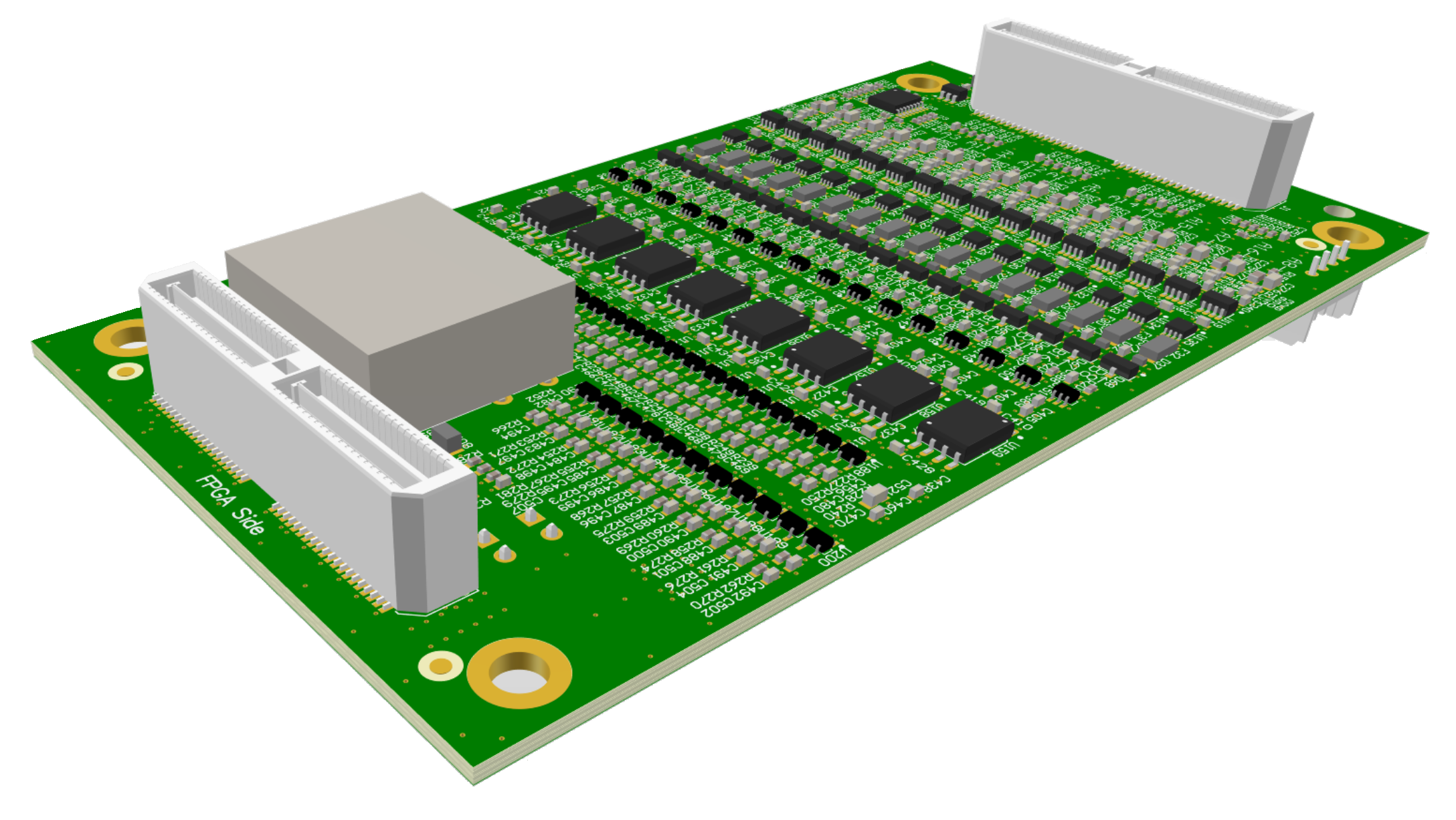
The OP5367 features a 32 channel digital input/output board. The output channels operating at 5 V (CMOS/TTL) or 3.3 V (LVTTL) and the input channels are high impedance with programmable high and low thresholds.
Main Features
The 32 input channels are grouped into four banks of 8 channels, each with independent thresholds per bank.
Digital In programmable threshold 0-50V.
The 32 output channels are configurable for either 5 V ±10% (CMOS/TTL Logic ) or 3.3 V (LVTTL).
Digital Out TTL, max output current: 32 mA/ch or 800 mA total combined
Low latency < 20 ns, High resolution of 10 ns with 100 MHz FPGA.
Galvanically isolation to real environment signals provides protection to the simulator from damaging voltages.
Channel Description
Digital Input
- Voltage
Voltage range 0-50V
Protection ±50VDC
Zin > 100kOhms
Programmable Vih and Vil on all the range per group of 8
>50 Mb/s, <30 ns of latency
...
Digital Output
Single Ended Output voltage, selected by dip which, for all output, 3.3 V / 5.0 V (LVTTL, TTL)
Short Circuit Protection
Protection ±50V DC/AC, for all channel at the same time
Current 24 mA
>50 Mb/s, <30 ns of latency
Theoretical
timing timing resolution: 10 ns (for FPGA at 100 MHz)
...
Configuration
Selection by BOM only of the direction, par group of 8:
Board |
Model | |
126-0616_32DOUT_TTL_TypeB | OP5367-1 |
126-0602_16DIN_Dual_Threshold_16DOUT_TTL_TypeB | OP5367-3 |
126-0604_32DIN_Dual_Threshold_TypeB | OP5367-5 |
Ouptut Voltage Selection
It is possible to select the output voltage of all channels for +3.3V (LVTTL) or +5.0V (TTL) operation via a dip switch installed on the OP5367.
| Background Color | ||||||||
|---|---|---|---|---|---|---|---|---|
| ||||||||
| Panel | ||||||||
| ||||||||
Make sure the simulator is powered downoff before actioning the dip switch |

See the location of the dip switch in the picture below: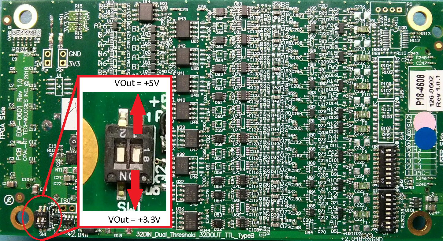
...
Typical Use Cases
The card is ideal for interfacing with devices operating at low voltage.
| Background Color | ||
|---|---|---|
| ||
| Note | ||
TTL signals are not recommended for long-distance data transmission.
| ||
| Background Color | color | #D3D3D3

| Info |
|---|
For compatibility of this card, please consult thethe Hardware compatibility chart. |