Documentation Home Page ◇ Hardware Home Page
Pour la documentation en FRANÇAIS, utilisez l'outil de traduction de votre navigateur Chrome, Edge ou Safari. Voir un exemple.
OP5300 Modules Handling
- Sylvain Ménard
The information below provides general guidelines for module handling.
See also:
Form Factor
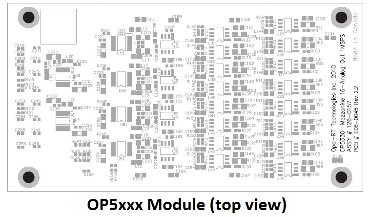
The OP5300 series of mezzanine modules follows OPAL-RT's Type-B form factor.
|
|
|---|
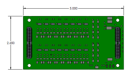
- The modules are rectangular in shape, their L x W dimensions are 6.60 cm x 12.50 cm (2.6” x 4.92”)
- Unless otherwise specified, the modules' height is 15mm (0.06")
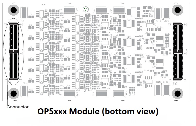
- Two Samtec Q Strip High-Speed 80pos connectors are located on the bottom side of the module's PCB. The connectors are labelled either J1/J2 or P1/P2:
- connector J2 (or P2): this connector carries signals to/from the FPGA: IDs, EEPROM signals, control data or measured data, 3.3/5V power signals.
- connector J1 (or P1): this connector carries signals to/from the external world: power signals (12/18V), data signals, etc.
- Four mounting holes allow to affix it to the carrier board of the real-time simulator with screws.
Installation
OP5300 modules come pre-installed on the carrier board of the real-time simulator. Follow these instructions to install a new module or to replace a defective module.
Should servicing be necessary due to a defective board or for configuration changes to the system, authorization must be requested from OPAL-RT before opening the system. Opening the unit without approval renders the warranty null and void.
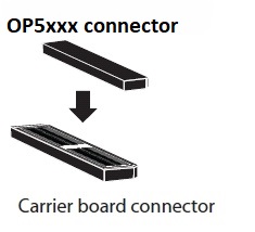
The module must be installed on the carrier board using great care. Use an electrostatic bracelet when manipulating the module.
The module can only be used with OPAL-RT’s carrier boards. Its location on the carrier board must match the expected location programmed in the FPGA chip of the simulator.
- Open the real-time chassis following the procedure provided by OPAL-RT when authorization for servicing was granted.
- Locate the carrier board, and locate the slot on the carrier where the module should be installed or replaced. Refer to the user manual of the system to identify the slots.
- Module removal
- Unscrew the four screws located at each corner of the module, and gently pull the module vertically out of the carrier board's connectors. Make sure to keep the plastic stand-offs connected to the carrier board.
- Unscrew the four screws located at each corner of the module, and gently pull the module vertically out of the carrier board's connectors. Make sure to keep the plastic stand-offs connected to the carrier board.
- Module installation
- Make sure the plastic stand-off is installed on the carrier,
- Turn the module in the proper direction so that its polarized connectors align with the carrier board connectors,
- Apply light pressure vertically to push the module into the carrier board. When the module is installed, only the top of the circuit board is visible. The four mounting holes should be vis-a-vis the plastic stand-offs,
- Use the four screws to affix the module to the carrier board for a secure connection.
Connection
Since the modules are located inside the I/O expansion chassis or the real-time simulator, their signals are not accessed by the user directly, but through dedicated DB37-F connectors made available at the back of the chassis. The module signals are routed to these connectors via the carrier board of the system.
Refer to the User Manual of your system to identify how the modules are mapped to the chassis's DB37-F connectors.
Each DB37-F connector typically provides connection points for 16 channels. Modules with 32 channels use 2 DB37-F connectors.
The pin assignment of the DB37-F connector varies depending on the type of module it is connected to.
To prevent damage, make sure to refer to the pin assignment of each specific module installed on your system before connecting the signals.
Calibration
Due to the nature of the electronic circuitry they use, the analog-to-digital and digital-to-analog modules are subject to a slight dispersion of the values they output or measure, as compared to the theoretical values.
To overcome this, the modules are factory-calibrated before being installed on the customer system. This calibration process is used to determine gain and offset parameter values to ensure that the module operates within the prescribed and acceptable range of values, typically with a maximum of ±20 mV around the expected value.
The gain and offset parameters obtained during the calibration process are stored in an EEPROM on the module. They are accessed at power up by the FPGA of the system to which the module is connected, and used during simulation to adjust the output or input values of the modules.
OPAL-RT TECHNOLOGIES, Inc. | 1751, rue Richardson, bureau 1060 | Montréal, Québec Canada H3K 1G6 | opal-rt.com | +1 514-935-2323
Follow OPAL-RT: LinkedIn | Facebook | YouTube | X/Twitter